Building a single-stage CPU in Ripes (Part 2 -- Memory and control instructions)
Previously: Single-stage CPU part 1
Next up: Five-stage CPU part 1
Step 4: Load instructions
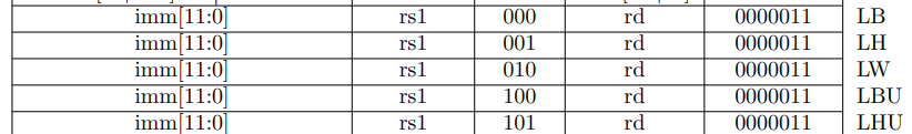
We can now easily implement LW, since the address computation is an I-type ADD instruction. There aren’t any new subcomponents to add, and we just have to make some connections to data memory and create a new input to the register data_in multiplexer. The memory controller itself does the sign-extend or 0-extend computation required for LB, LW, LBU, and LHU as long as we provide the correct control signal, so we get those operations for “free,” as well.
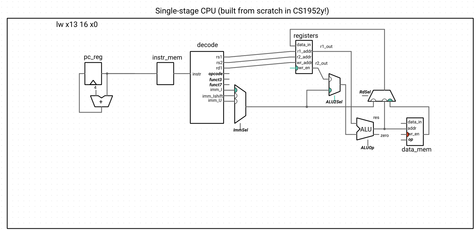
Updated CPU wiring
    // Data memory
    data_mem->mem->setMemory(m_memory);
    alu->res >> data_mem->addr;
    0 >> data_mem->data_in;
    0 >> data_mem->wr_en;
    control->mem_op >> data_mem->op;
Step 5: Store instructions
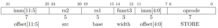
For a store, we have to add functionality for an S-type instruction to the decoder and controller, which involves the same type of code we’ve been writing already.

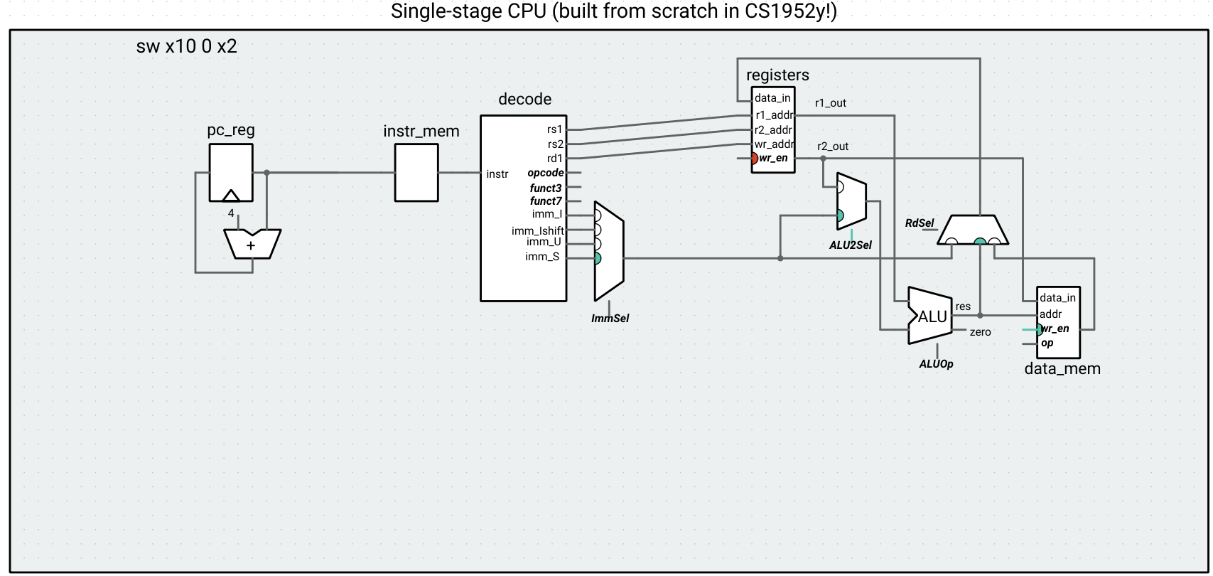
Up until this point, the wr_en signal of the register file has been hard-wired to 1, and the wr_en signal of the data memory has been hard-wired to 0, because all of the instructions we’ve encountered have written to a register and not written to memory. The store instruction does the opposite, so we need to update our controller with two outputs that get connected to these signals.
Controller wr_en logic for register file and data memory
    reg_w << [=] {
      switch (opcode.uValue()) {
      case 0b0010011: // register-immediate
      case 0b0110011: // register-register
      case 0b0110111: // LUI
      case 0b0000011: // load
        return 1;
      case 0b0100011: // store
      default:
        return 0;
      }
    }; // reg_w;

    mem_w << [=] { return opcode.uValue() == 0b0100011; }; // store
We can now run HW1d on our processor.
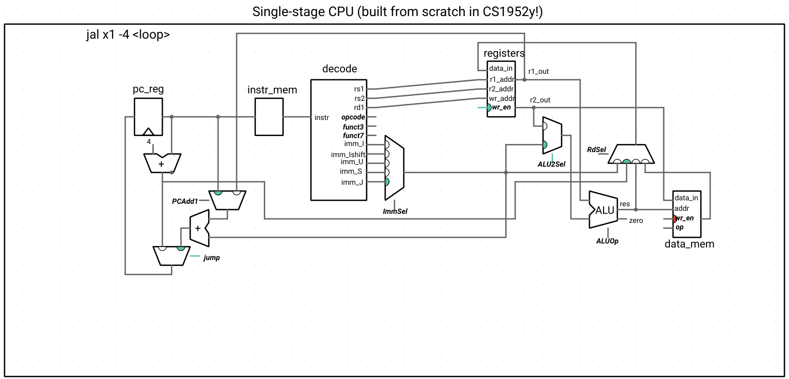
Step 6: Unconditional jumps
To implement control logic, we first work with the jump instructions, JAL and JALR. In a high-level programming language, function calls would be compiled into JAL or JALR instructions. The unlinked jump (J) does not appear in the RISC-V spec because it is a pseudo-instruction encoded as JAL with rd1 being x0 (so we do not implement it separately in hardware, since the assembler takes care of synthesizing it).
JAL and JALR have very similar behavior – both compute a new address for the PC using an immediate, and both write the value of the return address (pc + 4) to the rd register (which means we add another input to the RdSel mux). The difference is that JAL uses the current PC to compute the new address, and JALR uses the value in rs1 – this is the purpose of the PCAdd1 mux in the circuit below. Because they encode immediates differently (JALR needs to leave room for rs1 and is an I-type instruction, but JAL is not), we have to add some decoder logic for the J-type instruction. We also have to introduce a multiplexer that chooses what the next PC is, based on whether or not the instruction is a jump.
Warning: the RISC-V specification states that the LSB of the new PC address for JALR is ignored after the add (it is guaranteed to be 0 for JAL – verify for yourself that this is the case). Technically, we would need to enforce this in hardware in order for our computer to be safe, because an instruction like JALR x1, x0, 1 would try to write a value of 1 to the PC, which is an invalid instruction address because RISC-V instructions are on 2- or 4-byte boundaries depending on the extension. For simplicity’s sake, we will throw caution to the wind and trust that the compiler/assembly developer will supply properly aligned immediate operands to JALR (just don’t ship a CPU like this!).

The ALU isn’t used at all for our implementation of JAL and JALR – we could use the ALU to compute the new PC address, but instead, we choose to create a new adder (P&H does this as well). This is because branch instructions will also require us to compute a new PC address, and we will use the ALU to perform the various branch comparisons. Other implementations (such as the single-stage processor that comes with Ripes) choose to do it the other way, using the ALU to compute the new address and introducing a new unit for branching logic.
PC selection circuit
    registers->r1_out >> pc_add1->get(PCAdd1::RS); // JALR
    pc_reg->out >> pc_add1->get(PCAdd1::PC);       // JAL
    control->pc_add1 >> pc_add1->select;
    pc_add1->out >> pc_add->op1;
    imm_sel->out >> pc_add->op2;
    pc_inc->out >> pc_sel->get(PCSel::INC);
    pc_add->out >> pc_sel->get(PCSel::J);
    control->jump >> pc_sel->select;
Step 7: AUIPC

Now that we’re working more with the PC-related parts of the circuit, let’s implement AUIPC, which adds the immediate to the PC and stores the result in the destination register. We could implement this instruction either using the ALU or the adder we are using to compute jump addresses. Let’s do the first option, so that we don’t have to add logic to output the result of the PC adder to rd. This means adding a mux for the first input of the ALU. Check that the mux signals that are lit up in the picture below correspond with your understanding of the data that should be used for this instruction:
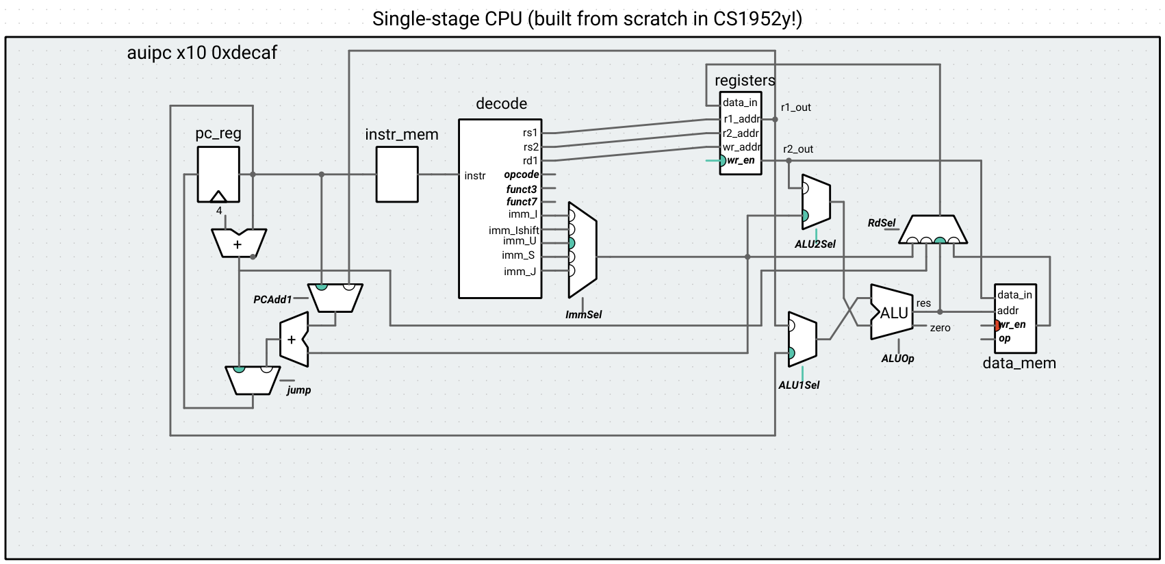
AUIPC allows the program to jump to instructions that are farther away than would be possible with just JAL and JALR. More information is given on page 16 of the RISC-V spec.
Step 8: Conditional branches
The remaining control transfer instructions are the conditional branches.
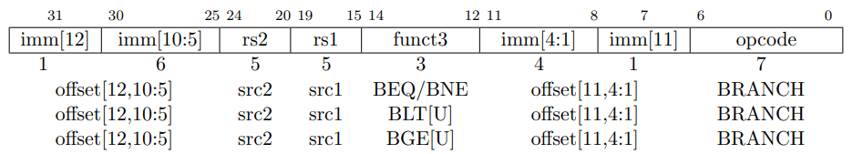
BGT, BGTU, BLE, and BLEU are pseudoinstructions synthesized as the opposite of BLT[U] and BGE[U].
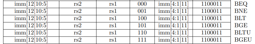
To perform the branch comparison for BLT and BGE, we can use the ALU with operation LT (directly for BLT, and inverted for BGE). To perform the branch comparison for BEQ/BNE, we use the ALU operation SUB to perform the equality check.
Updated ALU control for branching
    alu_ctrl << [=] {
      ...
      } else if (opcode.uValue() == 0b1100011) { // branches
        switch (funct3.uValue()) {
        case 0b000: // BEQ
        case 0b001: // BNE
          return ALUOp::SUB;
        case 0b100: // BLT
        case 0b101: // BGE
          return ALUOp::LT;
        case 0b110: // BLTU
        case 0b111: // BGEU
          return ALUOp::LTU;
        default:
          throw std::runtime_error("Invalid funct3 field");
        }
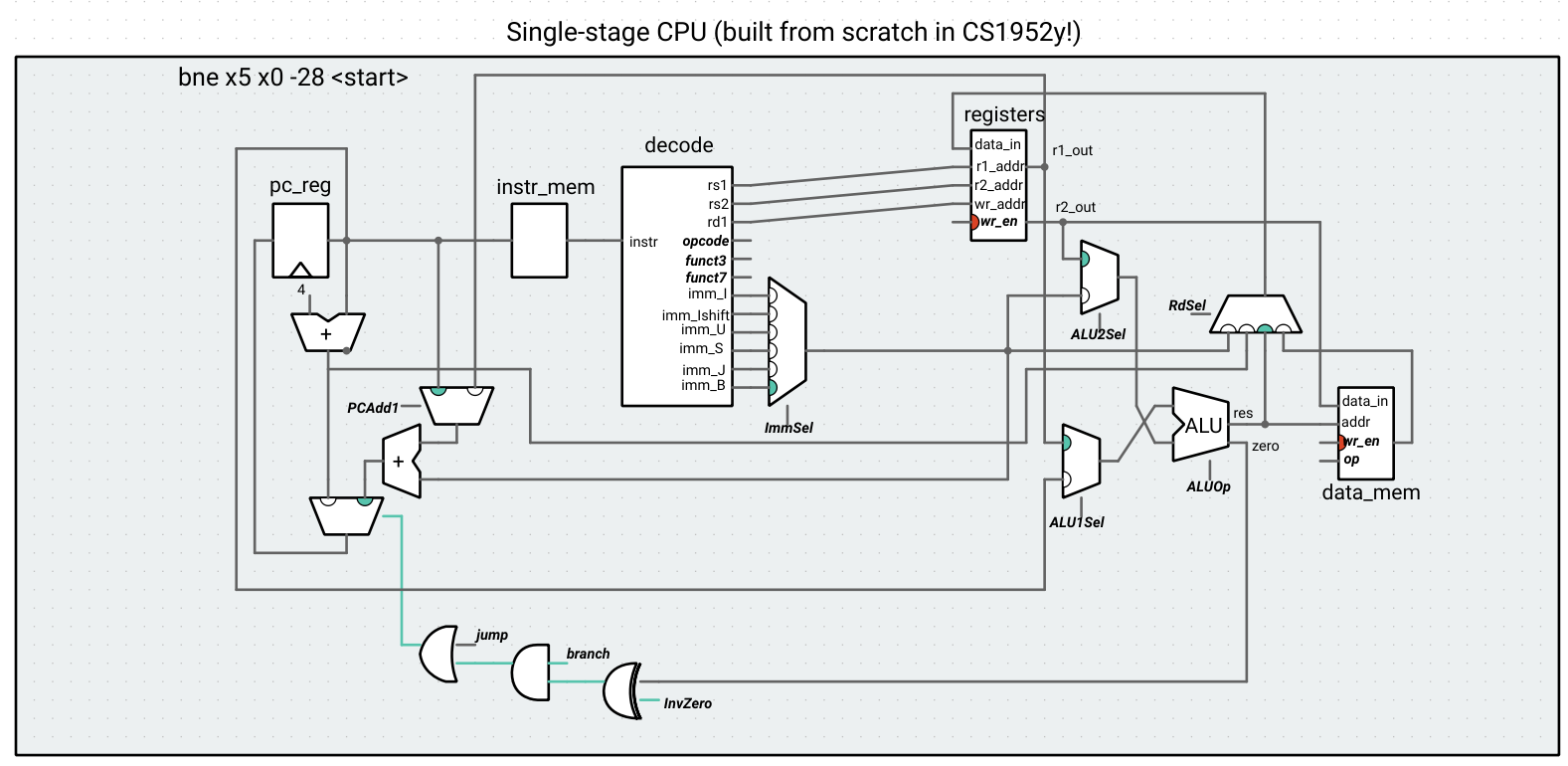
Instead of using the entire ALU result, all we need to know is if the output of the ALU is zero or non-zero, which justifies the zero signal we added to the ALU all the way in the beginning of this journey. Based on the operation, we need a control bit to either select or invert the zero-signal (for example, two numbers will be equal if the ALU output after subtracting is 0, so a BEQ branch will be taken when this signal is low, but a BNE branch will be taken when this signal is high). Instead of a multiplexer, an XOR gate can be used to invert a single bit.
Zero-bit inversion control
    inv_zero << [=] {
      if (opcode.uValue() == 0b1100011) { // Branches
        switch (funct3.uValue()) {
        case 0b000: // BEQ
        case 0b101: // BGE
        case 0b111: // BGEU
          return 0;
        case 0b001: // BNE
        case 0b100: // BLT
        case 0b110: // BLTU
          return 1;
        default:
          throw std::runtime_error("Invalid funct3 field");
        }
      } else {
        return 0; // don't care
      }
    }; // inv_zero
The input to the multiplexer that selects the PC has been changed to a logic gate circuit: if an instruction is a non-conditional jump OR if it’s a branch AND the branch should be taken according to the (possibly inverted) ALU zero signal, then the next PC comes from the adder with the immediate. Otherwise, it’s just the next sequential instruction (PC + 4).
We have now implemented a basic RV32I CPU! If we had done this in hardware, we would have a working computer.
You may be realizing that, at any given time, large parts of this circuit are sitting idle as electrical signals travel from the PC register, to instruction memory, to the decoder, to control logic, to the ALU, to the data memory, to the RdSel and PC selection muxes. In fact, while we have a working CPU, we could do better in terms of performance by allowing all of the units to be used in parallel for different instructions. This is called pipelining, and we will explore it next lecture.